1 of 5
112099
FEATURES
Automatically restarts microprocessor after
power failure
Maintains active-high reset for 350 ms after
V
CC
returns to an in-tolerance condition
Accurate 5%, 10% or 15% microprocessor 5V
power supply monitoring
Reduces need for discrete components
Precision temperature-compensated voltage
reference and voltage sensor
Low-cost TO-92 package or surface mount
SOT-223 package
Internal 5k pull-up resistor
Operating temperature of -40
∞
C to +85
∞
C
PIN ASSIGNMENT
PIN DESCRIPTION
PIN 1
Ground
PIN 2
Reset
PIN 3
V
CC
PIN 4
Ground (SOT-223 only)
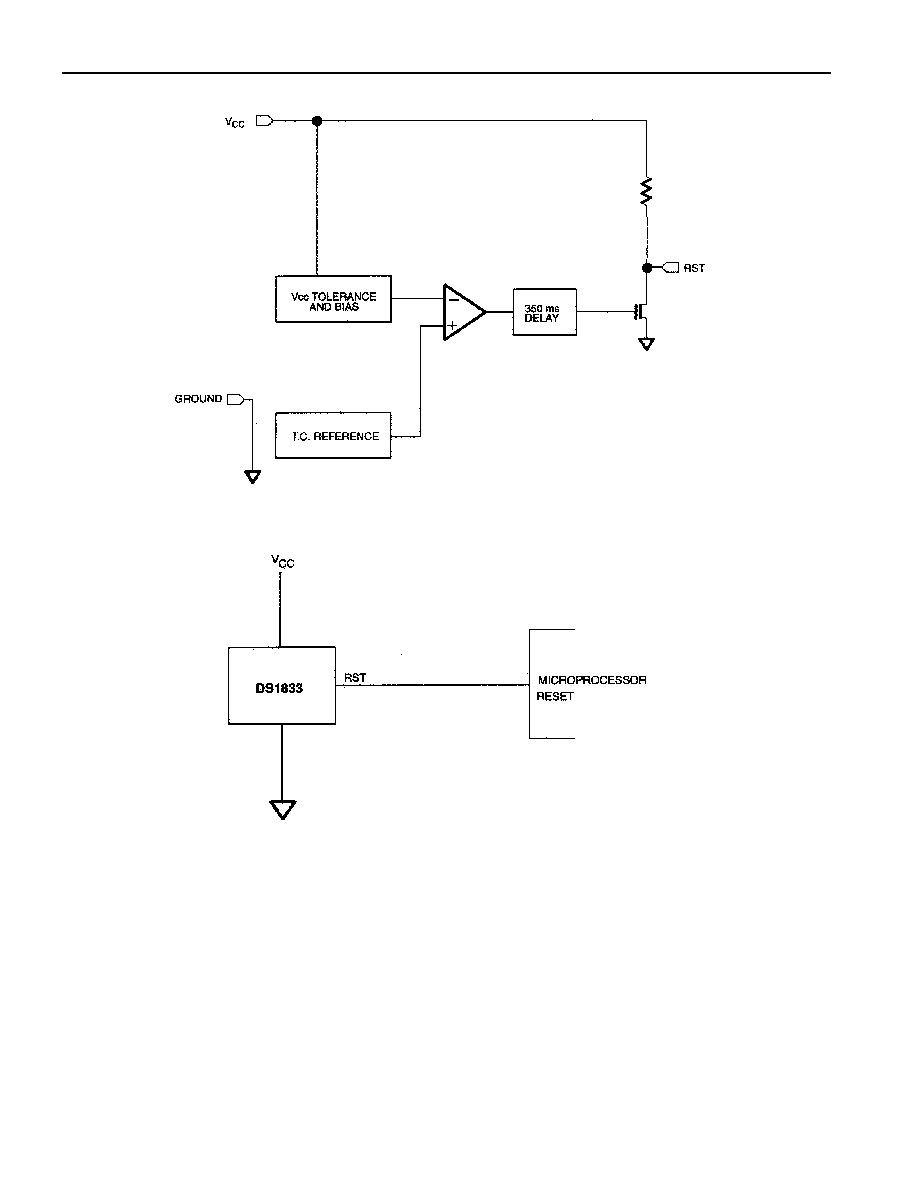
DESCRIPTION
The DS1833 EconoReset uses a precision temperature compensated reference and comparator circuit to
monitor the status of the power supply (V
CC
). When an out-of-tolerance condition is detected, an internal
power fail signal is generated which forces reset to the active (high) state. When V
CC
returns to an in-
tolerance condition, the reset signal is kept in the active state for approximately 350 ms to allow the
power supply and processor to stabilize.
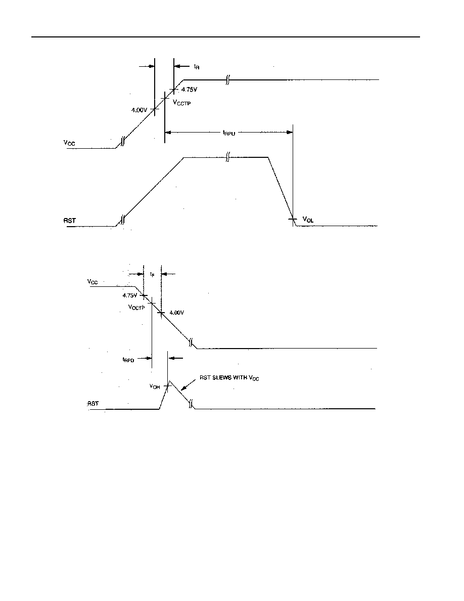
OPERATION - POWER MONITOR
The DS1833 provides the functions of detecting out-of-tolerance power supply conditions and warning a
processor-based system of impending power failure. When V
CC
is detected as out-of-tolerance, as
defined by the tolerance of the part selected, the RST signal is asserted. On power-up, RST is kept active
for approximately 350 ms after the power supply has reached the selected tolerance. This allows the
power supply and microprocessor to stabilize before RST is released.
DS1833
5V EconoReset
www.dalsemi.com
1 2 3
1 2 3
TO-92 PACKAGE
See Mech.
Drawings Section
2
3
4
SOT-223 PACKAGE
See Mech.
Drawings Section
1
DALLAS
DS1833
DS1833
4 of 5
ABSOLUTE MAXIMUM RATINGS*
Voltage on V
CC
Pin Relative to Ground
-0.5V to +7.0V
Voltage on I/O Relative to Ground
-0.5V to V
CC
+0.5V
Operating Temperature
-40
∞
C to +85
∞
C
Storage Temperature
-55
∞
C to +125
∞
C
Soldering Temperature
260
∞
C for 10 seconds
*
This is a stress rating only and functional operation of the device at these or any other conditions
above those indicated in the operation sections of this specification is not implied. Exposure to
absolute maximum rating conditions for extended periods of time may affect reliability.
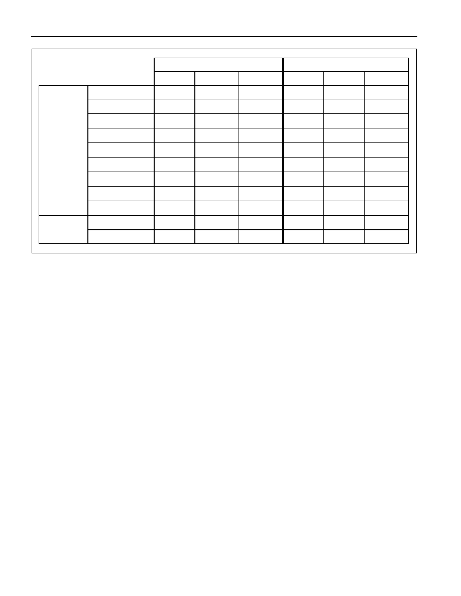
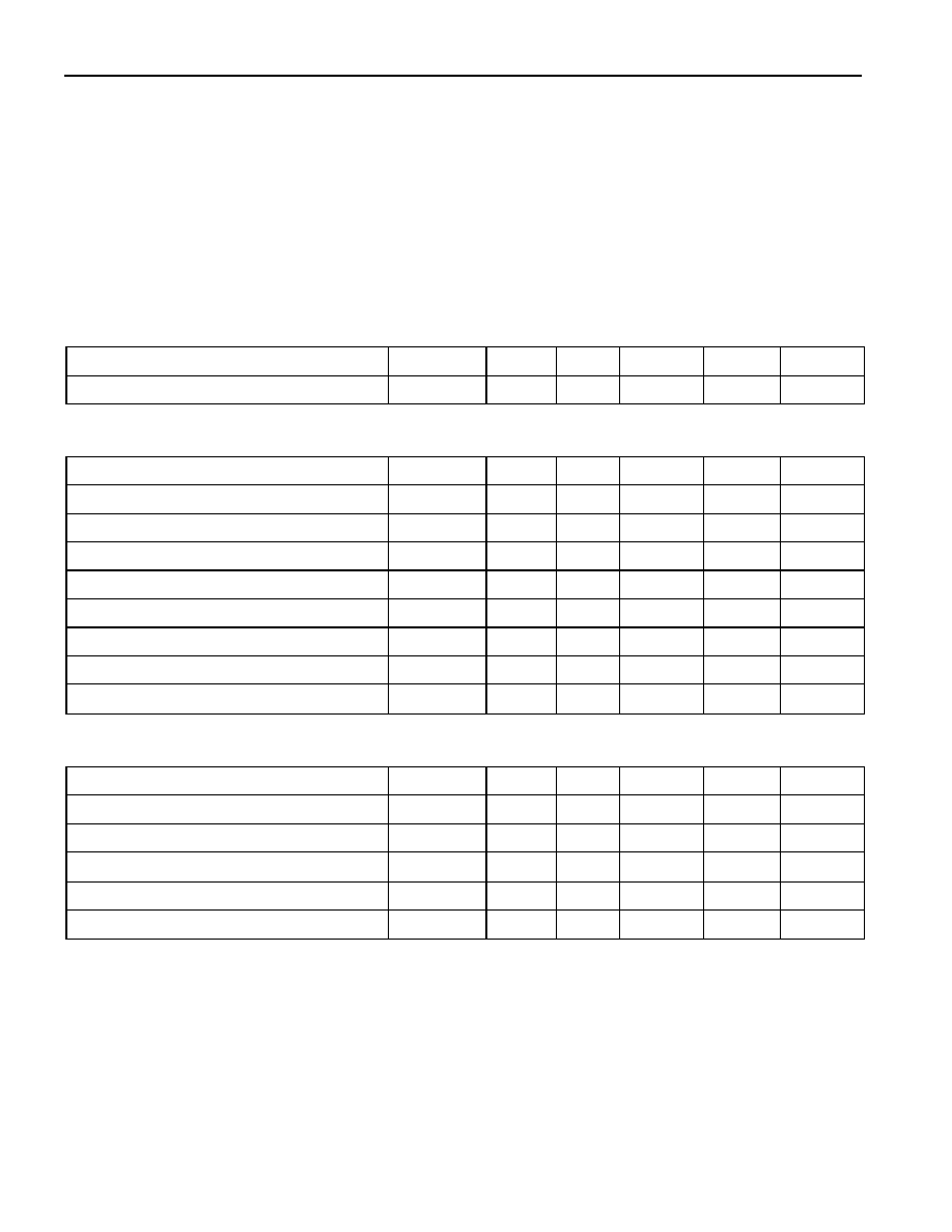
RECOMMENDED DC OPERATING CONDITIONS (-40
∞
C to +85
∞
C)
PARAMETER
SYMBOL
MIN
TYP
MAX
UNITS NOTES
Supply Voltage
V
CC
1.2
5.0
5.5
V
1
DC ELECTRICAL CHARACTERISTICS (-40
∞
C to +85
∞
C; V
DD
=5V
±
10%)
PARAMETER
SYMBOL
MIN
TYP
MAX
UNITS NOTES
Low Level @ RST
V
OL
0.4
V
1
Output Current @ 0.4V
I
OL
+8
mA
Operating Current
I
CC
1.5
2
mA
V
CC
Trip Point 5%
V
CCTP1
4.5
4.625
4.74
V
1
V
CC
Trip Point 10%
V
CCTP2
4.25
4.375
4.49
V
1
V
CC
Trip Point 15%
V
CCTP3
4.0
4.125
4.24
V
1
Output Capacitance
C
OUT
10
pF
Internal Pull-Up Resistor
R
P
3.75
5
6.25
k
AC ELECTRICAL CHARACTERISTICS (-40
∞
C to +85
∞
C; V
CC
=5V
±
10%)
PARAMETER
SYMBOL
MIN
TYP
MAX
UNITS NOTES
Reset Active Time
t
RST
250
350
450
ms
V
CC
Detect to RST
t
RPD
100
ns
V
CC
Slew Rate (4.75V - 4.00V)
t
F
300
µ
s
V
CC
Slew Rate (4.00V - 4.75V)
t
R
0
ns
V
CC
Detect to RST
t
RPU
250
350
450
ms
NOTES:
1.
All voltages are referenced to ground.